|
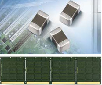
- Designers of electronic equipment are faced with ever increasing requirements for size reduction and increased functionality. These are easily achieved by smaller components capable of improved performance. Samsung Electro-Mechanics introduces the world highest capacitance 1uF MLCC for 0201 case sizes, replacing 0402 case sizes in IT and industrial applications.
High capacitance is achieved by effective control over sub-micron layers, from ultra-fine starting powders to firing. Finer grains result in better performance under DC-bias and aging testing. In addition to mounting space savings, lower ESL effectively reduces high frequency noise in most applications, such as mobile phone, note-PC, GPS, etc.
- The package substrate is used to transfer electrical signals between a semiconductor chip and a main board. Chip Scale Package(CSP) and its package size is not larger than 1.2 times that of the chip area. The chip is connected to a substrate by two types of bonding, wire-bonding and flip-chip bonding. Gold wire is used for wire-bonding and solder ball is used for flip chip packaging. CSP is mainly used for packaging high-end semiconductors, such as memory for computers, mobile devices, PDA, etc.
|