|
Established in 1980, Hanmi semiconductor has grown up as one of the leading global companies manufacturing equipment in the fields of semiconductors, PVs, LEDs and PCBs. The company covers all processes such as design, development, fabrication, assembly, installation, training, and after-sales service, thus ensuring the highest quality. The company also steadily develops and commercializes upgraded versions of semiconductor equipment utilizing its own software and SECS/GEM communications.
With more than 200 globally competitive engineers and constant investment in R&D, the company is leading the technology for semiconductor equipment ahead of the market trends, thereby establishing solid partnerships with many major companies across the world.
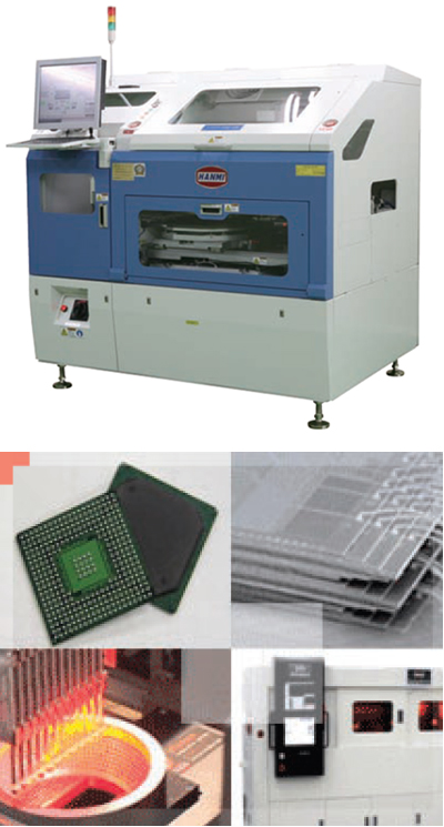
For the flip chip packages which replace the wire bonding technologies, flip chip bonder attaches wafer DIE to the substrate directly. It is high technology that requires excellent accuracy and supreme vision inspection. With the market trend requiring semiconductor packages with more high-density, demand for the company¡¯s flagship flip chip bonder is increasing.
The company¡¯s flagship flip chip bonder, actively marketed under the brand name of flip chip bonder 200c, is winning good approval in both domestic and overseas markets, with its considerably enhanced features including providing high speed & high-accuracy bonding service for flip chip, machine accuracy of ¡¾7§@3sigma, ideal productivity of 10,000 UPH, etc.
With its most advanced X-Y-Z motion control for bonding head and dual flipper & bonder, high productivity is ensured.
The capability of precise pick up & bonding process by supreme vision inspection with PRS function is also basically available. Prealignment stage for higher real productivity is supported.
|