|
Since its establishment in 2003, OptoPAC has specialized in developing and producing WLP (Wafer-Level Packaging) for CMOS or CCD Image Sensors as a venture company.
Backed by its patented specific technology and know-how in the field of image sensor packaging, the maker is currently focusing on maximizing the production of its best-quality products, constantly investing in R&D in the field.
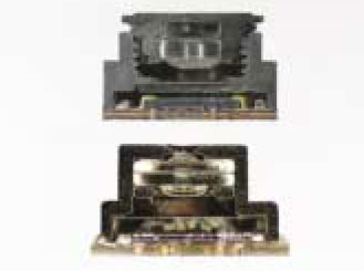
The maker¡¯s NeoPAC WLP is designed for image sensors. It utilizes a glass wafer on which at least one patterned metal layer and one patterned passivation layer is fabricated.
During the operation, the image sensor is attached to the metal layer using IP chip solder joints. Larger solder balls are used to connect the product to a PCB or ex-circuit.
Normally, it is characterized by a simple structure that achieves high yield and low cost through the use of standard and proven fabrication processes.
It can be applied to many such areas as camera phones, PC and laptop cameras, digital cameras, camcorders, etc. Of special note, in comparison to the existing methods of COB, CLCC and PLCC, it can provide customers with reliable products in terms of lower costs and smaller size.
|